


|
|


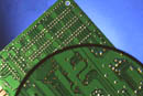
Schematic Capture and PCB Layout
HED uses Accel EDA V14 CAD software and provides in-house Schematic Capture
and PCB (Printed Circuit Board) Layout. For high density designs HED uses the Mentor
Graphics Suite for tight control over impedance matching and trace lengths.
Our CAD systems allow us to develop Multilayer Boards
using Leaded or Surface Mount technology. The customer is supplied all Gerber and NCD Drill
File information as well as all schematics, parts lists, and assembly drawings.
|
|
|
|